Circuit Diagram Of 3 Input Ttl Nand Gate 74ls10 Triple 3-inp
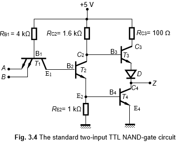
Working principle of the two-input ttl nand gate Circuit diagram of two input ttl nand gate Understanding digital buffer, gate, and logic ic circuits
[DIAGRAM] Ladder Logic Diagram Nand Gate - MYDIAGRAM.ONLINE
Ttl xor gate circuit diagram Nand-gate| digital logic gates || electronics tutorial Ic gate logic input nand three diagram triple circuits buffer understanding digital part functional figure
Unit 04 logic families and semiconductor memories
Electronic – input and output impedance of a ttl nand gate – valuable¿cómo funcionan las puertas ttl nand? Ttl inverter diagramTtl circuit: transistor -transistor logic circuit operation.
74hc00 / 74hct00, quad 2Q4) the circuit diagram of a ttl nand gate is illustrated with a set of Ttl transistor nand logicElectronic – ttl logic gate resistor values – valuable tech notes.

Transistor-transistor logic (ttl)
Input ttl nand p10 assuming3 input and gate circuit diagram Pinout input nand ic datasheet logic triple74ls10 triple 3-input nand logic gate ic.
2 input nand gate circuit diagramA ttl 2-input nand gate breadboard circuit. Why does the ttl family use a totem pole circuit on the output[diagram] ladder logic diagram nand gate.

Circuit diagram of 2 input ttl nand gate
3 input nand gate circuit diagram2 input nand gate layout A 4-input ttl nand gate and its circuit symbolCircuit diagram of two input ttl nand gate.
Unit 04 logic families and semiconductor memoriesA close up of a mapdescription automatically generated Introduction to nand gateTtl nand gate schematic.

Solved: figure p10.50 shows a three-input ttl nand gate. assumi
Ttl nand gate circuit diagramNand gate diagram 74hc00 ttl input quad 7400 pinout latch using gates nor push pull funny four has 3 input ttl nand gate circuitTtl xor gate circuit diagram.
Nand gate electronics input digital logic ttl gates tutorial pole three configuration totem transistor .

![[DIAGRAM] Ladder Logic Diagram Nand Gate - MYDIAGRAM.ONLINE](https://i.pinimg.com/originals/ab/24/18/ab24187cb2417e3dd37e2b074fda32ea.png)